

Description
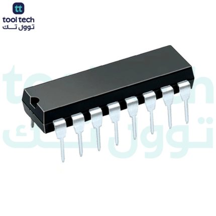
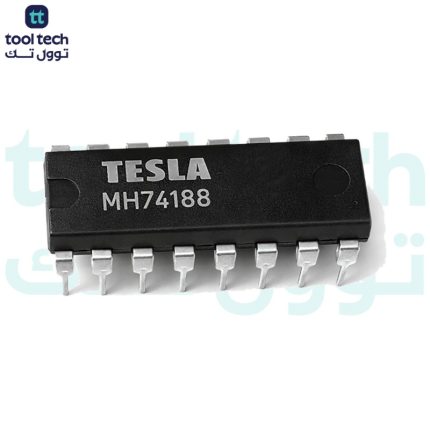
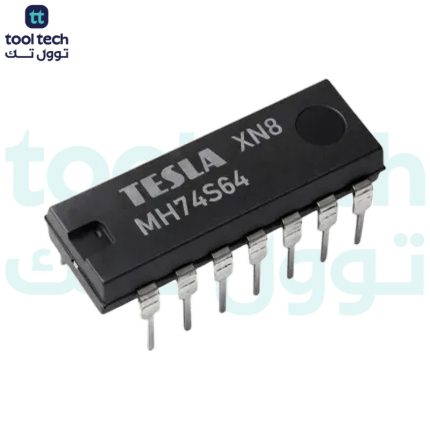
7434
Buffer & line Driver
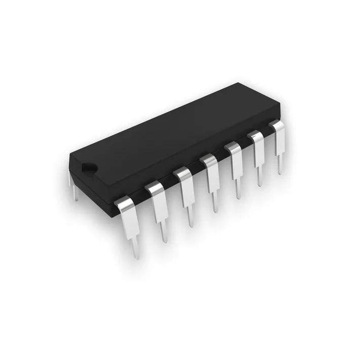
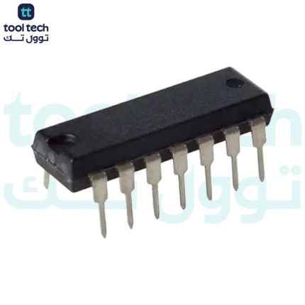
6V 2μA IC PDIP-14
The 7434 is a hex buffer IC containing six independent non-inverting buffers in a single package. It is designed to interface TTL-level signals with CMOS circuits, ensuring compatibility and signal integrity in mixed-logic systems. The HC version operates with a supply voltage range of 2V to 6V, making it suitable for 5V systems while retaining the low power consumption and high noise immunity typical of CMOS technology.
This device is characterized for operation over a wide temperature range, meeting both industrial and military specifications. It provides strong output drive capability, capable of driving up to 10 LS-TTL loads, and includes diode protection on all inputs to guard against electrostatic discharge (ESD) and voltage spikes.
Features:
Six independent non-inverting buffer/driver gates.
Improves signal strength and fan-out capability.
Isolates logic stages to protect sensitive circuits.
TTL-compatible logic levels.
Suitable for driving long traces and multiple loads.
Specifications:
SYMBOL
PARAMETER
TEST CONDITION
VCC (V)
MIN.
TYP.
MAX.
UNIT
VIH
HIGH level input Voltage
2.0
1.5
V
4.5
3.15
V
6.0
4.2
V
VIL
LOW level input voltage
2.0
0.3
V
4.5
0.9
V
6.0
1.2
V
VOH
HIGH level output voltage
VIN = VIH or VIL, IOH = -20μA
2.0
1.9
2.0
1.9
V
VIN = VIH or VIL, IOH = -20μA
4.5
4.4
4.5
4.4
V
VIN = VIH or VIL, IOH = -20μA
6.0
5.9
6.0
5.9
V
VIN = VIH or VIL, IOH = -4mA
4.5
3.98
4.3
V
VIN = VIH or VIL, IOH = -5.2mA
6.0
5.48
5.2
V
VOL
LOW level output voltage
VIN = VIH or VIL, IOL = 20μA
2.0
0.1
V
VIN = VIH or VIL, IOL = 20μA
4.5
0.1
V
VIN = VIH or VIL, IOL = 20μA
6.0
0.1
V
IIN
Input leakage Current
VIN = VCC or GND
6.0
0.1
μA
ICC
Quiescent Supply Current
VIN = VCC or GND, Iout = 0μA
6.0
2
20
μA
Pinout:
Pin
Name
Function
1
1A
Input for Buffer 1
2
1Y
Output for Buffer 1
3
2A
Input for Buffer 2
4
2Y
Output for Buffer 2
5
3A
Input for Buffer 3
6
3Y
Output for Buffer 3
7
GND
Ground
8
4Y
Output for Buffer 4
9
4A
Input for Buffer 4
10
5Y
Output for Buffer 5
11
5A
Input for Buffer 5
12
6Y
Output for Buffer 6
13
6A
Input for Buffer 6
14
VCC
Supply Voltage
Applications:
TTL-to-CMOS level conversion.
Signal buffering in bus-oriented systems.
Input/output port isolation in microcontrollers.
Driving high-capacitance or long trace lines.
General-purpose non-inverting buffer in digital designs.
Packages:
1x 7434 Buffer & line Driver 6V 2μA IC PDIP-14.
Documents:
GD74HC34 Datasheet.














Reviews
There are no reviews yet.