


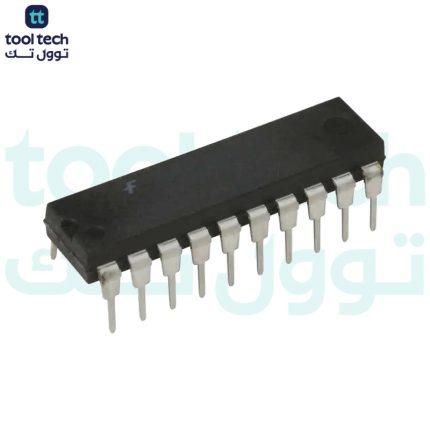
Description
74533 High Speed
CMOS
Logic Octal Inverting Transparent Latches with 3-State Outputs 5V 8µA IC PDIP-20
The 74533 is a high-speed CMOS octal inverting transparent latch with common latch-enable (LE) and common three-state output-enable (OE) controls. While LE is asserted the eight inputs (D0–D7) pass through to the outputs. OE places all outputs into high-impedance when asserted, allowing easy bus sharing and hot-swapping of devices on a common data bus. The device is manufactured in HC/HCT silicon-gate CMOS technology to provide low static power consumption and TTL/LSTTL compatibility in the HCT variant.
Designed as a rugged bus-interface component, the 74533 features buffered inputs and three-state outputs capable of driving multiple LSTTL loads, balanced transition times, and operation over a wide temperature range. It’s available in multiple package options (PDIP, SOIC, CERDIP) for through-hole and surface-mount assembly, and its independent LE/OE controls make it convenient for gating, register staging, and temporary data storage in microprocessor systems, address/data multiplexing, and glue-logic applications.
Features:
Common latch-enable (LE) control for all eight channels.
Common three-state output-enable (OE) control for bus sharing.
Buffered inputs for clean signal capture.
Three-state outputs for bus-line driving and multiplexing.
Inverting transparent latch architecture.
74533 Low power CMOS construction (HC/HCT families).
Designed for easy interfacing with TTL/LSTTL (HCT variant).
Specifications:
Parameter
Value / Range
Supply Voltage (HC)
2.0V to 6.0V
Supply Voltage (HCT)
4.5V to 5.5V
Propagation Delay
~13ns (at 5V)
Input Leakage Current
±0.1µA
Three-State Leakage Current
±0.5µA
Quiescent Supply Current
Very low (CMOS technology)
Input Capacitance
~10pF
Output Capacitance
~20pF
Operating Temperature Range
−55°C to +125°C
Output Drive Capability
Drives multiple LSTTL loads
Pinout:
Pin
Name
Function
Pin
Name
Function
1
OE
Output Enable
20
Vcc
Supply Voltage
2
Q0
Inverted Output 0
19
Q7
Inverted Output 7
3
D0
Data Input 0
18
D7
Data Input 7
4
D1
Data Input 1
17
D6
Data Input 6
5
Q1
Inverted Output 1
16
Q6
Inverted Output 6
6
Q2
Inverted Output 2
15
Q5
Inverted Output 5
7
D2
Data Input 2
14
D5
Data Input 5
8
D3
Data Input 3
13
D4
Data Input 4
9
Q3
Inverted Output 3
12
Q4
Inverted Output 4
10
GND
Ground
11
LE
Latch Enable
Applications:
Bus-line buffering and bus sharing (three-state outputs).
Temporary data storage / register staging in microprocessor systems.
Address/data multiplexing and bus arbitration.
Glue logic / interface between CMOS and TTL systems (HCT variant).
Packages:
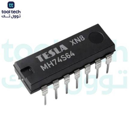
1x 74533 High Speed CMOS Logic Octal Inverting Transparent Latches with 3-State Outputs 5V 8µA IC PDIP-20.
Documents:
CD74HC533 Datasheet.
















Reviews
There are no reviews yet.