


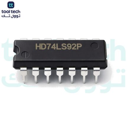
Description
Pin layout
74LS90 Pin Configuration
Pin No.
Pin Name
Description
1
CLKB
Clock Input 2
2
R1
Reset 1
3
R2
Reset 2
4
NC
Not Connected
5
Vcc
Positive Supply Input
6
R3
Reset 3
7
R4
Reset 4
8
Qc
Output Pin 3
9
Qb
Output Pin 2
10
Gnd
Ground
11
Qd
Output Pin 4
12
Qa
Output Pin 1
13
NC
Not Connected
14
CLKA
Clock Input 1
Features and Specifications
Typical power dissipation: 45mW
High count rates: 42MHz
Choice of counting modes
Input Clamp Diodes Limit High-Speed Termination Effect
Supply voltage: 5V
Operating Ambient Temperature Range: –55 to 125°C
Brief About 7490 IC
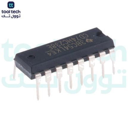
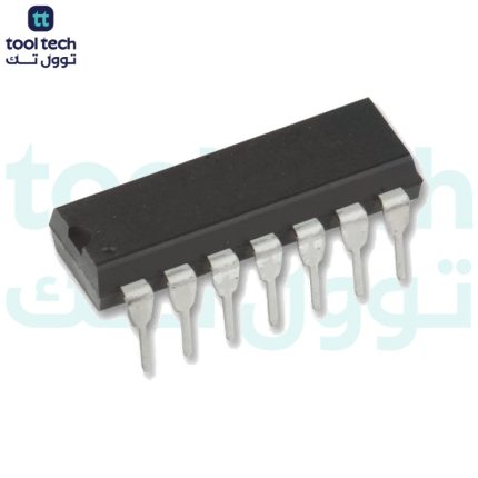
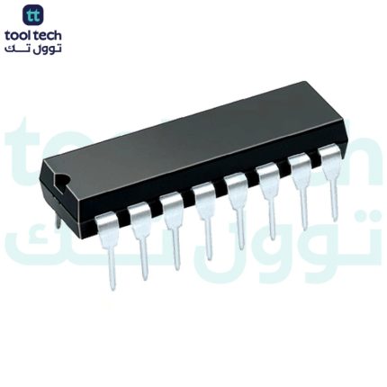
74LS90
is basically a MOD-10 decade counter that generate a BCD output code. It consists of four master-slave JK flip-flop, which are internally connected to provide MOD-2 (count to 2) counter and MOD-5 counter. 74LS90 also have an independent toggle JK flip-flop by CLKA and other three are driven by the CLKB.
Internal Logic Diagram
How to Use Decade Counter IC?
The below circuit diagram is for
BCD decade counter
, by giving HIGH and LOW logic to the CLKA pin, IC start counts from zero to 8 at every HIGH logic. If you want to display the number on a 7-segment display you need a seven segment display driver IC.
74LS90 BCD Counter IC Datasheet















Reviews
There are no reviews yet.