


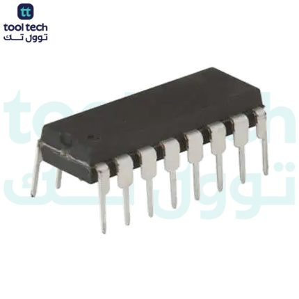

Description
7400 IC Quad 2-Input NAND Gate
7400
is a member of the 74XXYY IC series. The 74xxyy ICs are
logic gates
of digital electronics.
7400 IC
has four
NAND gates
. Also, each gate has two inputs. Hence name QUAD TWO INPUT NAND GATE.
7400 Pin Configuration
7400 is a 14-PIN device. The chip is available in different packages and is chosen depending on requirements. The description for each pin is given below.
Pin Number
Description
NAND GATE 1
1
A1-INPUT1 of GATE 1
2
B1-INPUT2 of GATE 1
3
Y1-OUTPUT of GATE1
NAND GATE 2
4
A2-INPUT1 of GATE 2
5
B2-INPUT2 of GATE 2
6
Y2-OUTPUT of GATE2
NAND GATE 3
9
A3-INPUT1 of GATE 3
10
B3-INPUT2 of GATE 3
8
Y3-OUTPUT of GATE3
NAND GATE 4
12
A4-INPUT1 of GATE 4
13
B4-INPUT2 of GATE 4
11
Y4-OUTPUT of GATE4
SHARED TERMINALS
7
GND- Connected to ground
14
VCC-Connected to positive voltage to provide power to all four gates
7400 Features and Specifications
Product Attribute
Attribute Value
Product Category:
Logic Gates
Logic Function:
NAND
Logic Family:
74HC
Number of Gates:
4 Gate
Number of Input Lines:
8 Input
Number of Output Lines:
4 Output
High-Level Output Current:
– 5.2 mA
Low-Level Output Current:
5.2 mA
Propagation Delay Time:
7 ns
Supply Voltage – Max:
6 V
Supply Voltage – Min:
2 V
Minimum Operating Temperature:
– 40 C
Maximum Operating Temperature:
+ 125 C
Package/Case:
PDIP-14
Function:
NAND
Logic Type:
Quad NAND Gate
Operating Supply Voltage:
2 V to 6 V
How To Use This Chip
Like every other chip in the 7400 series, this IC must be connected to power before you can use it. Most 7400 ICs support a VCC voltage of 5V. One difference between the HC and LS version of the chip is that the 74HC04 supports 2V to 6V, while the 74LS04 supports only 5V.
Once it’s connected, you can use any of the six inverters inside.
Where 7400 IC is Used?
There are many reasons for using 7400 in electronic circuits. Here are a few examples where it is used.
7400 basically used for performing the NAND function. The IC has four NAND gates in it. Each gate can be used separately.
When you want a logic inverter. NAND gates in this chip can be reconfigured to make them NOT gates. So we can make 7400 a four-not gate chip if necessary.
Where high-speed NAND operation is necessary. This chip has less transition times which are needed for high-speed applications. So 7400 can be used in high-frequency systems.
7400 is one of the cheapest ICs. It is really popular and is available everywhere.
How to Use 7400 IC
Like every other chip in the 7400 series, this IC must be connected to power before you can use it. Most 7400 ICs support a VCC voltage of 5V. One difference between the HC and LS version of the chip is that the 74HC00 supports 2V to 6V, while the 74LS00 supports only 5V.
Once connected, you can use any of the four basic NAND gates inside.
Now it is good to remind you that NAND gate is a combination of AND gate and NOT gate.
So NAND = AND + NOT.
The
truth table of the NAND gate
is given as,
Input1
Input2
AND Output
NAND Output
LOW
LOW
LOW
HIGH
HIGH
LOW
LOW
HIGH
LOW
HIGH
LOW
HIGH
HIGH
HIGH
HIGH
LOW
To understand the NAND gate responses let us study the internal circuitry of the NAND gate.
In the circuit when both inputs A1 and B1 are LOW:
Both transistors Q1 and Q2 will be OFF. So the total supply voltage appears across the transistors Q1 and Q2. Because output Y1 is nothing but voltage across transistors Q1 and Q2, Y1 will be HIGH.
In the case when any one input is HIGH:
Only the relative transistor will be ON leaving the other OFF. With that, the entire supply voltage appears across the transistor which is in the OFF state. Because output Y1 is voltage across both transistors Q1 and Q2, Y1 will be HIGH.
When both inputs are HIGH:
Both transistors will be ON and the voltage across both of them will be zero. Because output Y1 is voltage across both transistors Q1 and Q2, Y1 will be LOW.
After verifying the cases, you can tell that we have satisfied the above truth table. The output equation for the NAND gate can be given as, Y=AB.
Now let us consider a simple application circuit of the chip NAND gate.
Here we have connected two inputs to two buttons and the output is connected to an LED. The output logic of the gate can be known by the ON and OFF states of this LED.
Under normal circumstances, both buttons are not pressed and are open. With that, both inputs of the gate will be LOW. When both inputs are LOW, the output will be HIGH according to the truth table discussed above. Since output is HIGH the LED will turn ON.
In case one of the buttons is closed. One input will be LOW and the other will be HIGH. Even in this case, the output will be HIGH according to the truth table. Since output is HIGH the LED will turn ON.
Only when both buttons are pressed we will have LOW output turning the LED OFF.
With these three cases, we have realized the truth table for chip NAND gate. We can use all four gates this way to satisfy our needs.
Applications
General purpose logic
Digital Electronics
PCs and notebooks
Servers
ALUs
Networking
Digital systems
Component Datasheet
7400 Datasheet














Reviews
There are no reviews yet.