
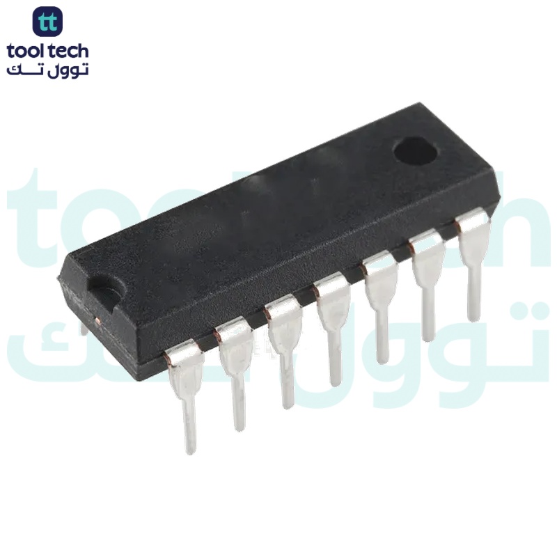

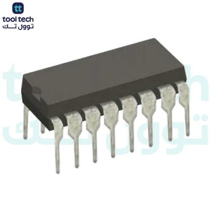
Description
74107 Dual JK
Flip-Flop IC
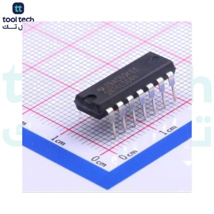
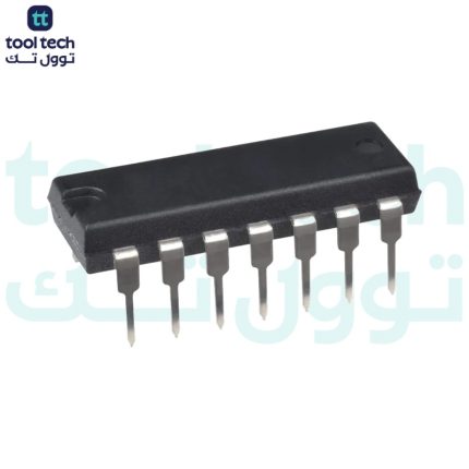
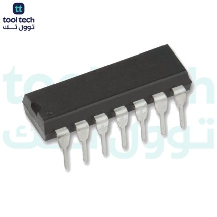
DIP-14 – Reliable Digital Memory
The 74HC107 is a JK Flip-Flop with individual J, K, Direct Clear, and Clock Pulse inputs. Output changes are initiated by the HIGH-to-LOW transition of the clock. The J and K inputs must be stable one setup time prior to the high-to-low clock transition for predictable operation. The 74HC107 IC has a wide range of working voltage, and a wide range of working conditions, and directly interfaces with CMOS, NMOS, and TTL.
What is a JK Flip-Flop?
The JK Flip Flop is basically a gated RS flip flop with the addition of the clock input circuitry. When both the inputs S and R are equal to logic “1”, the invalid condition takes place. Thus to prevent this invalid condition, a clock circuit is introduced. The JK Flip Flop has four possible input combinations because of the addition of the clocked input. The four inputs are “logic 1”, ‘logic 0”. “No change’ and “Toggle”.
Features:
Dual JK flip-flop configuration for versatile logic operations
Standard DIP-14 package for easy integration into circuits
Used for memory storage, pulse generation, and toggling applications
Ideal for synchronous digital systems and timing circuits
Specifications
Product Attribute
Attribute Value
Product Category:
Flip Flops
Number of Circuits:
2
Logic Family:
HC
Logic Type:
J-K Type Flip-Flop
Polarity:
Inverting, Non-Inverting
Input Type:
CMOS, LVTTL
Output Type:
Differential
Propagation Delay Time:
170 ns
High-Level Output Current:
– 5.2 mA
Low-Level Output Current:
5.2 mA
Supply Voltage – Min:
2 V
Supply Voltage – Max:
6 V
Minimum Operating Temperature:
– 55 C
Maximum Operating Temperature:
+ 125 C
Mounting Style:
Through Hole
Package / Case:
PDIP-14
Packaging:
Tube
Function:
JK Type
Number of Channels:
2
Number of Input Lines:
2
Number of Output Lines:
1
Operating Supply Voltage:
2 V to 6 V
Operating Temperature Range:
– 55 C to + 125 C
Product Type:
Flip Flops
Quiescent Current:
4 uA
Reset Type:
Reset
74HC107 Pin Configuration
Pin No
Pin Name
Description
1
J1
Input Pin J1
2
Q1
Active high Output pin 1
3
Q1′
Active low Output pin 1
4
K1
Input Pin K1
5
Q2
Active high Output pin 2
6
Q2′
Active low Output pin 2
7
GND
Ground Pin
8
J2
Input Pin J2
9
CP2
Clock Pulse Input Pin 2
10
CD2
Reset Pin 2
11
K2
Input Pin K2
12
CP1
Clock Pulse Input Pin 1
13
CD1
Reset Pin 1
14
VCC
Supply Voltage
74HC107 Pinout:
Applications
They are used in digital clocks, electronic meters, and other electronic devices that
display
numerical information.
Document:
Data sheet















Reviews
There are no reviews yet.