


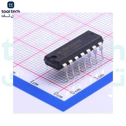
Description
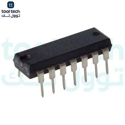
74126 Features
Quad Bus Buffers with 3-State Outputs
Separate Control for each Channel
High-Impedance Output State
Standard TTL Switching Voltages
Specifications:
Product Attribute
Attribute Value
Product Category:
Buffers & Line Drivers
Logic Family:
LS
Number of Input Lines:
4 Input
Number of Output Lines:
4 Output
Polarity:
Non-Inverting
Package/Case:
PDIP-14
High Level Output Current:
– 2.6 mA
Low Level Output Current:
24 mA
Quiescent Current:
36 mA
Supply Voltage – Min:
4.75 V
Supply Voltage – Max:
5.25 V
Operating Supply Current:
62 mA
Minimum Operating Temperature:
0 C
Maximum Operating Temperature:
+ 70 C
Function:
Buffer/Line Driver
Input Signal Type:
Single-Ended
Logic Type:
Bipolar
Number of Channels:
4 Channel
Operating Supply Voltage:
4.75 V to 5.25 V
Output Type:
3-State
Product Type:
Buffers & Line Drivers
Propagation Delay Time:
18 ns at 5 V
Series:
SN74LS126A
Subcategory:
Logic ICs
Technology:
Bipolar
Note:
Like every other chip in the 74 series, this IC must be connected to power before you can use it. Most 74126 ICs support a VCC voltage of 5V. One difference between the HC and LS version of the chip is that the 74HC126 supports 2V to 6V, while the 74LS126 supports only 5V.
74126 Pinout Diagram
74126 Pin Description
Pin No
Pin Name
Description
1
1G, 1G*’
LOW/High pin of Buffer 1
2
1A
Input Of Buffer 1
3
1Y
Output Of Buffer 1
4
2G,2G*’
LOW/High pin of Buffer 2
5
2A
Input Of Buffer 2
6
2Y
Output Of Buffer 2
7
GND
Ground
8
3Y
Output Of Buffer 3
9
3A
Input Of Buffer 3
10
3G,3G*’
LOW/High pin of Buffer 3
11
4Y
Output Of Buffer 4
12
4A
Input Of Buffer 4
13
4G,4G*’
LOW/High pin of Buffer 4
14
VCC
Positive Supply
Applications
A
digital buffer
(or a voltage buffer) is an electronic circuit element used to isolate input from the output.
Datasheet













Reviews
There are no reviews yet.