


Description
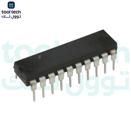
The 74HC373 high speed octal D-type latches utilize advanced silicon-gate CMOS technology. They possess the high noise immunity and low power consumption of standard CMOS integrated circuits, as well as the ability to drive 15 LS-TTL loads. Due to the large output drive capability and the 3-STATE feature, these devices are ideally suited for interfacing with bus lines in a bus organized system.
When the LATCH ENABLE input is HIGH, the Q outputs will follow the D inputs. When the LATCH ENABLE goes LOW, data at the D inputs will be retained at the outputs until LATCH ENABLE returns HIGH again. When a high logic level is applied to the OUTPUT CONTROL input, all outputs go to a high impedance state, regardless of what signals are present at the other inputs and the state of the storage elements. The 74HC logic family is speed, function, and pin-out compatible with the standard 74LS logic family. All inputs are protected from damage due to static discharge by internal diode clamps to VCC and ground.
Features:-
Typical propagation delay: 18 ns
Wide operating voltage range: 2 to 6 volts
Low input current: 1 µA maximum
Low quiescent current: 80 µA maximum (74 Series)
Output drive capability: 15 LS-TTL loads
Specifications:-
Parameter
Specification
Supply Voltage (VCC
− 0.5 to + 7.0V
Input Voltage (VIN)
−1.5VCC + 1.5V
Output Voltage (VOUT)
− 0.5 to VCC + 0.5V
Clamp Diode Current (IIK, IOK)
± 20 mA
DC Output Current, per pin (IOUT)
± 35 mA
DC VCC or GND Current, per pin (ICC)
± 70 mA
Storage Temperature Range (TSTG)
− 65°C to + 150°C
Power Dissipation (PD) (Note 4)
600 mW
S.O. Package only
500 mW
Lead Temperature (TL) (Soldering 10 seconds)
260°C
Related Document:-
74HC373 IC Datasheet















Reviews
There are no reviews yet.