


Description
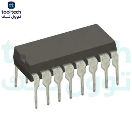
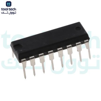
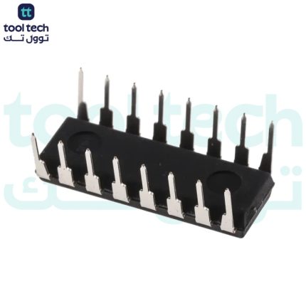
4015 IC
Shift Register
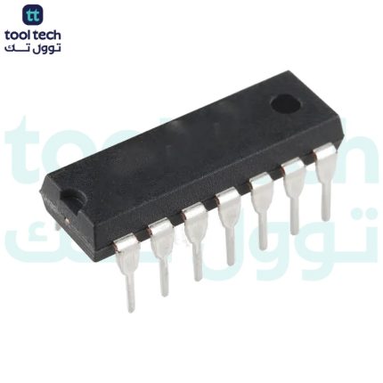
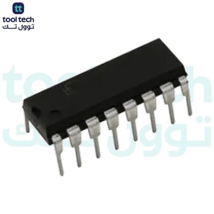
Serial to parallel PDIP-16 Original
The
CD4015B
is a monolithic CMOS integrated circuit that functions as a dual 4-bit static shift register. Its primary role is to convert serial data into parallel data, operating as a serial-in, parallel-out (SIPO) register. The device is constructed using complementary MOS technology, which provides it with the classic benefits of very low power consumption and a wide operating voltage range. This makes it a versatile and robust building block for various digital logic systems, capable of interfacing with both CMOS and TTL logic families when operated at a suitable voltage.
The IC contains two identical and completely independent shift registers on a single chip. Each register has its own dedicated data input, clock input, and a master reset input, allowing for flexible and separate control. Data presented at the serial input is shifted into the register on the low-to-high transition of the clock pulse. The master reset input, when set to a high logic level, asynchronously clears all stages of its respective register, forcing all outputs to a low state, regardless of the clock or data input conditions.
Each of the four stages in a register is represented by a Q output, providing parallel access to the shifted data. The data bit moves from one stage to the next with each clock pulse, effectively creating a delay line or a means to hold multiple bits of data. This parallel output structure is ideal for tasks like driving multiple outputs from a single serial data line, such as illuminating LEDs or controlling other digital loads, thereby reducing the number of microcontroller I/O pins required in a system.
Features:
Dual 4-Stage Static Shift Registers.
Serial Input, Parallel Output Operation.
Master Reset for Each Register.
Medium-Speed Operation.
Fully Static Operation (Does not require a minimum clock frequency).
Low Power TTL Compatibility.
Standardized Symmetrical Output Characteristics.
100% Tested for Quiescent Current at 20V.
Pin Overview:
Pinout for the 4015 IC
Pin Name
Pin #
Type
Description
VDD
16
Power
Supply Voltage (+3 to +15V)
GND
8
Power
Ground (0V)
D
A
7
Input
Data pin for register A
CLK
A
9
Input
Clock pulse for register A
RST
A
6
Input
Reset pin for register A
Q
A0
,Q
A1
,Q
A2
,Q
A3
5,4,3,10
Output
4-bit output for register A
D
B
15
Input
Data pin for register B
CLK
B
1
Input
Clock pulse for register B
RST
B
14
Input
Reset pin for register B
Q
B0
,Q
B1
,Q
B2
,Q
B3
11,12,13, 2
Output
4-bit output for register B
Specifications:
Physical
Case/Package
PDIP
Contact Plating
Gold
Mount
Through Hole
Number of Pins
16
Technical
Direction
Unidirectional
Frequency
17 MHz
Input Capacitance
5 pF
Logic Function
Shift Register
Max Operating Temperature
125 °C
Max Supply Voltage
18 V
Min Operating Temperature
-55 °C
Min Supply Voltage
3 V
Number of Bits
4
Number of Bits per Element
4
Number of Circuits
2
Number of Elements
2
Number of Input Lines
1
Number of Output Lines
4
Power Dissipation
500 mW
Propagation Delay
400 ns
Quiescent Current
100 µA
Turn-On Delay Time
400 ns
Applications:
Serial-to-Parallel Data Conversion.
Data Storage and Temporary Memory.
Time Delay Circuits.
Sequence Generation and Control.
LED Matrix or Bar Graph Drivers.
Package Contents:
1x
4015 IC Shift Register Serial to parallel PDIP-16 Original
Datasheet













Reviews
There are no reviews yet.