

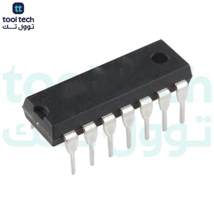
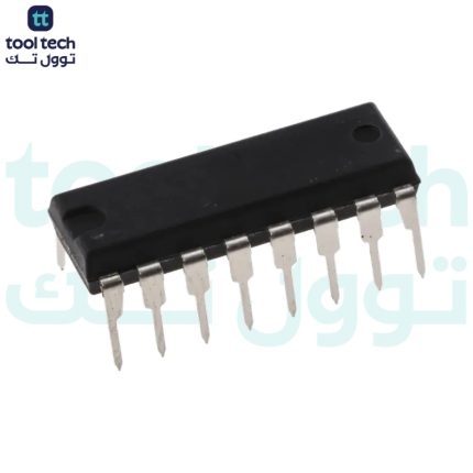
Description
4093 – An IC with Four Schmitt Trigger NAND Gates
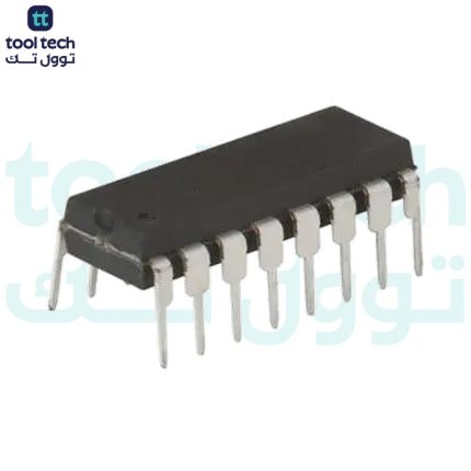
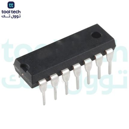
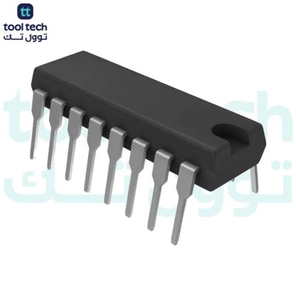
The 4093 is a CMOS chip with four NAND gates with a Schmitt trigger. Because each gate has two inputs and has four gates inside, it’s often referred to as a
Quad 2-Input NAND Schmitt Trigger
.
A NAND gate with a Schmitt trigger works more or less like a normal NAND gate. With the exception that the threshold for when it switches from LOW to HIGH is different from when it switches from HIGH to LOW.
Pin Overview
Pin Name
Pin #
Type
Description
VDD
14
Power
Supply Voltage (+3 to +15V)
GND
7
Power
Ground (0V)
A1 to A4
1, 5, 8, 12
Input
Inputs A of the four NAND gates
B1 to B4
2, 6, 9, 13
Input
Inputs B of the four NAND gates
Q1 to Q4
3, 4, 10, 11
Output
Outputs from the four NAND gates
Pin overview for the 4093 IC
What is a NAND gate with Schmitt Trigger?
First of all, a NAND gate is a logic gate that works like an AND gate with a NOT gate on the output. Therefore it’s often called NOT-AND.
A NAND gate built from AND and NOT gates
This means that a NAND gate gives a LOW output only when all inputs are HIGH as shown in the truth table below.
Input A
Input B
Output Q
0
0
1
1
0
1
0
1
1
1
1
0
Truth Table for the NAND gate
Schmitt Trigger
But this is a Schmitt trigger NAND gate. What does that mean?
This has to do with at what voltage the gate will interpret the input as a LOW or a HIGH input:
For example for a normal (non-Schmitt Trigger) gate that is powered from 5V, the gate might say that any voltage above 2.5V is HIGH, and any voltage below 2.5V is LOW. So if the input is at 2.5V and swinging a bit up and down (as these signals tend to do), then the output would be uncertain.
2.5V would be the
threshold voltage
.
But for a Schmitt trigger gate, the threshold voltage is different based on if the input changes from LOW to HIGH or from HIGH to LOW.
For example, if the input is currently LOW, then a Schmitt trigger gate might require the input voltage to go above for 3.5V to switch to HIGH. But when it has switched to HIGH, dropping a bit below 3.5V doesn’t matter. Because in order to switch back to LOW, the Schmitt trigger gate requires the input to go down below for example 1.5V.
Technical Specifications
Physical
Case/Package
PDIP
Contact Plating
Gold
Mount
Through Hole
Number of Pins
14
Technical
High Level Output Current
-4.2 mA
Logic Function
NAND, Schmitt Trigger
Low Level Output Current
4.2 mA
Max Operating Temperature
125 °C
Max Output Current
6.8 mA
Max Supply Voltage
18 V
Manufacturer Package Identifier
J (R-GDIP-T**)
Min Operating Temperature
-55 °C
Min Supply Voltage
3 V
Number of Bits
4
Number of Channels
4
Number of Circuits
4
Number of Elements
4
Number of Gates
4
Number of Input Lines
2
Number of Inputs
2
Number of Output Lines
1
Number of Outputs
1
Output Current
6.8 mA
Propagation Delay
130 ns
Quiescent Current
20 µA
Schmitt Trigger Input
Yes
Termination
Through Hole
Turn-On Delay Time
380 ns
4093 Datasheet

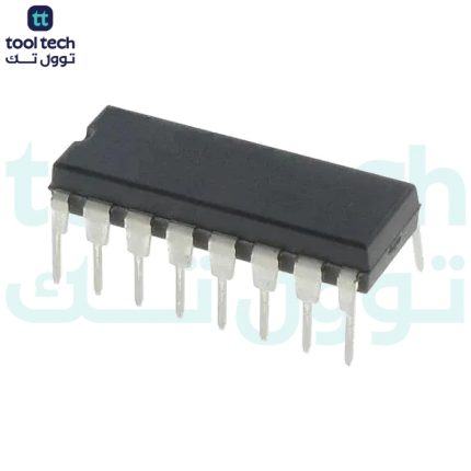
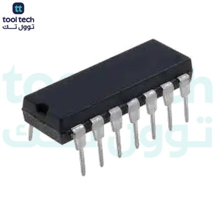













Reviews
There are no reviews yet.