


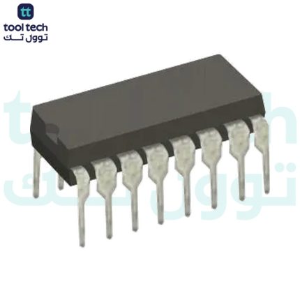

Description
Features:
• Wide Range of Digital and Analog Signal Levels
– Digital: 3 V to 20 V
– Analog: ≤20 VP-P
• Low ON Resistance,125 Ω (Typical) Over 15 VP-P Signal Input Range for VDD – VEE = 18 V
• High OFF Resistance, Channel Leakage of ±100pA (Typical) at VDD – VEE = 18 V
• Logic-Level Conversion for Digital Addressing Signals of 3 V to 20 V (VDD – VSS = 3 V to 20 V) to Switch Analog Signals to 20 VP-P (VDD – VEE = 20 V) Matched Switch Characteristics, rON = 5 Ω (Typical) for VDD – VEE = 15 V Very Low Quiescent Power Dissipation Under All Digital-Control Input and Supply Conditions, 0.2 μW (Typical) at VDD – VSS = VDD – VEE = 10 V
• Binary Address Decoding on Chip
• 5 V, 10 V, and 15 V Parametric Ratings
• 100% Tested for Quiescent Current at 20 V
• Maximum Input Current of 1 μA at 18 V Over Full Package Temperature Range, 100 nA at 18 V and 25°C
• Break-Before-Make Switching Eliminates Channel Overlap
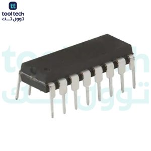
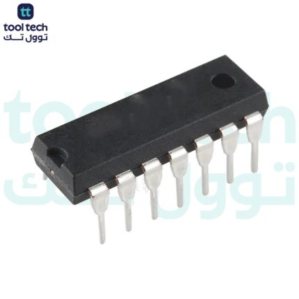
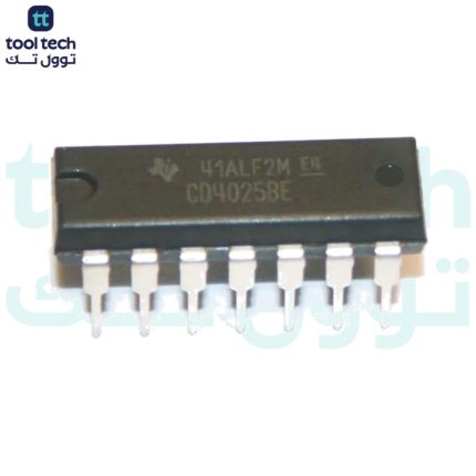
CD4051 Pinout
Pin No
Pin Name
Description
1
I/O 4
channel 4 i/o
2
I/O 6
channel 6 i/o
3
O/I
common i/o
4
I/O 7
channel 7 i/o
5
I/O 5
channel 5 i/o
6
INHIBIT
disable all channel
7
VEE
Emitter supply
8
VSS
source supply
9
C
input c
10
B
input b
11
A
input a
12
I/O 3
channel 3 i/o
13
I/O 0
channel 0 i/o
14
I/O 1
channel 1 i/o
15
I/O 2
channel 2 i/o
16
VDD
Drain supply
4051 Datasheet














Reviews
There are no reviews yet.